Here are the PCB design guidelines, when starting a new design, most of the time is spent on PCB circuit design and component selection, the PCB layout routing stage is often not well thought out due to inexperience.
Failure to provide sufficient time and effort for the PCB layout and routing phase of the design can lead to problems in the manufacturing phase or defects in functionality when the design is translated from the digital domain to physical reality.
What is the key to designing a board that is realistic and reliable on paper and in physical form? Let’s explore the first 6 PCB design guidelines you need to know when designing a manufacturable, functionally reliable PCB.
PCB design guidelines 1. Fine-tune your component placement
The component placement phase of the PCB layout process is both a science and an art, requiring strategic consideration of the major components available on the board.
While this process can be challenging, the way you place your electronic components will determine how easy your board is to manufacture and how well it meets your original design requirements.
While there is a general order to component placement, such as sequential placement of connectors, printed circuit board mounting devices, power circuits, precision circuits, critical circuits, etc., there are some specific guidelines to keep in mind, including
Orientation – Ensuring that similar components are positioned in the same direction will help to achieve an efficient and error-free soldering process.
Placement – Avoid placing smaller components behind larger components, which may be affected by the soldering of larger components and cause mounting problems.
Organization – It is recommended that all surface mount (SMT) components are placed on the same side of the board and that all through-hole (TH) components are placed on top of the board to minimize assembly steps.
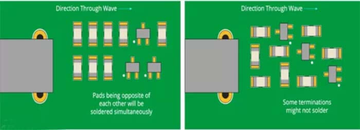
PCB design guidelines’ Good chip component orientation (left) and bad chip component orientation (right)
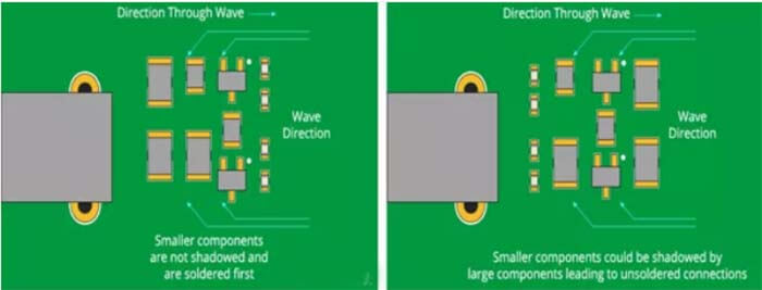
PCB design guidelines’ Good component arrangement (left) and bad component arrangement (right)
Other PCB design guidelines to be aware of, i.e. when using mixed technology components (through-hole and surface mount components), PCB manufacturers may require additional processes to assemble the board, which will increase your overall costs.
PCB design guidelines 2. Proper placement of power, ground, and signal routing
After placing the components, the power, ground, and signal routing can then be placed to ensure that your signals have a clean and trouble-free path of travel. At this stage of the layout process, please bear in mind some of the following PCB design guidelines.
PCB design guidelines 2.1. Locating the power and earth plane layers
It is always recommended to position the power and ground plane layers inside the board while keeping them symmetrical and centered. This helps to prevent your board from bending, which also relates to the correct positioning of your components.
For powering ICs, it is recommended to use a common path for each power supply to ensure a robust and stable alignment width and to avoid daisy-chaining power connections from component to component.
PCB design guidelines 2.2. Signal line routing
Next, connect the signal lines according to the design in the schematic. It is recommended to always take the shortest possible path and direct path alignment between components.
If your components need to be fixed in a horizontal orientation without any deviation, it is recommended to route the components on the board essentially horizontally where they come out and then vertically afterward.
This way the components will be fixed in a horizontal orientation as the solder migrates during soldering. This is shown in the upper part of the diagram below. The signal alignment in the bottom half of the diagram may cause the component to deflect as the solder migrates during soldering.
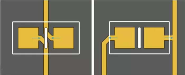
PCB design guidelines suggested PCB wiring mode (arrow indicates the direction of solder flow)
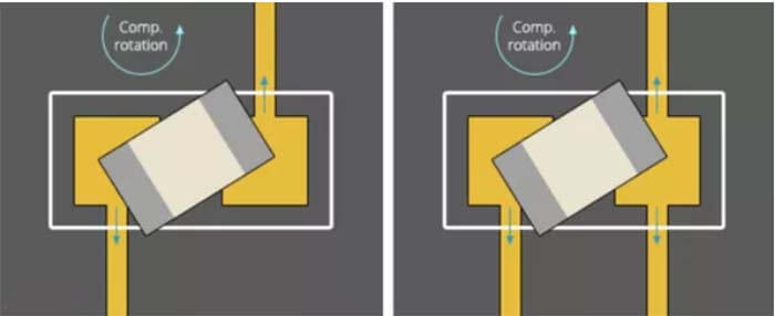
PCB design guidelines not recommend PCB wiring method (arrow indicates the direction of solder flow)
PCB design guidelines 2.3. Defining the network width
Your design may require different networks that will carry various currents, which will determine the required network width. With this basic requirement in mind, a width of 0.010” (10 mils) is recommended for low-current analog and digital signals.
When the PCB line current exceeds 0.3 amps, it should be widened. A free line width calculator is available here to make this conversion process easy.
PCB design guidelines 3. Effective isolation
You may have experienced how large voltage and current spikes in power supply circuits can interfere with your control circuitry for low voltage currents. To minimize such interference problems, follow these guidelines.
Isolation – Ensure that you keep power and control grounds separate for each power supply circuit. If you must connect them together in a PCB, make sure it is as close to the end of the power path as possible.
Placement – If you have placed a ground plane on the middle layer, make sure you place a small impedance path to reduce the risk of any power circuit interference and to help protect your control signals. The same guidelines can be followed to keep your digital and analog separate.
Coupling – To reduce capacitive coupling due to the placement of a large ground plane and the alignment above and below it, try to cross the analog ground only through the analog signal lines.
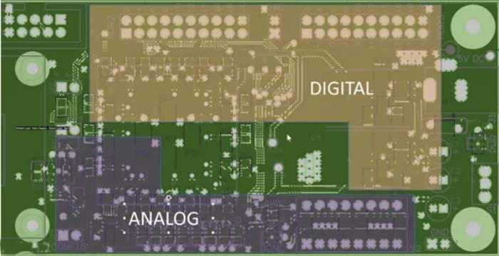
PCB design guidelines PCB component Isolation Example (Digital and Simulation)
PCB design guidelines 4. Solving heat problems
Have you ever had a circuit performance degradation or even board damage due to heating problems? There have been many problems that have plagued many designers due to a failure to consider heating dissipation. Here are some guidelines to remember to help solve heat dissipation problems.
PCB design guidelines 4.1. Identify troublesome components
The first step is to start considering which components will dissipate the most heat from the board. This can be done by first finding the “thermal resistance” rating in the component’s datasheet and then following the recommended guidelines for transferring the heat generated.
Heat sinks and cooling fans can be added to keep component temperatures down and remember to keep critical components away from any high heating sources.
PCB design guidelines 4.2. Adding hot air pads
The addition of hot air pads is useful for producing manufacturable boards, they are essential for high copper content components and wave soldering applications on multi-layer boards. As it is difficult to maintain process temperatures, it is always recommended to use hot air pads on through-hole components in order to make the soldering process as easy as possible by slowing down the rate of heat dissipation at the component pins.
As a general guideline, always use the hot air pad method of connection for any through-hole or over-hole connected to the ground plane or power plane. In addition to hot air pads, you can also add teardrops at the location of the pad connection line to provide additional copper foil/metal support. This will help to reduce mechanical and thermal stresses.
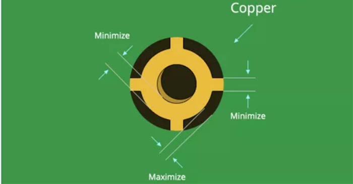
Typical hot air welding connection
PCB design guidelines 5. Hot air pad science
Many factories are responsible for the process SMT technology engineers often encounter circuit board components occurring empty solder, de-wetting, or cold solder, and so on this kind of solder cannot be solder (non-wetting) bad problems, no matter how to change the process conditions or reflow soldering furnace temperature No matter how much the process conditions are changed or how much the reflow oven temperature is adjusted, there is still a certain rate of non-wetting. Why does this happen?
Most of these soldering defects actually come from the board’s wiring (layout) design, and the most common is in the components of a few solder pins connected to a large area of copper, resulting in these components’ solder pins after reflow soldering occurring poorly, some hand-soldered components may also be due to similar circumstances and cause false soldering or welding problems, and some even because the heating is too long and the components to be soldered off. Some of them are even damaged due to long heating.
In general, PCBs often require large areas of copper foil for power (Vcc, Vdd, or Vss) and ground (GND, Ground) during circuit design. These large areas of copper foil are usually connected directly to the pins of some control circuits (ICs) and electronic components.
Unfortunately, if we want to heat these large areas of copper foil up to the temperature of molten tin, it usually takes longer than a separate solder pad (i.e. it heats up slower) and dissipates heat faster.
When such large areas of copper foil are connected to small components such as small resistors and capacitors at one end, but not at the other, soldering problems can occur due to inconsistent melting and solidification times.
If the temperature profile of the reflow solder is not adjusted properly and the preheating time is not sufficient, the solder pins of these components connected to a large area of copper foil will easily fail to reach the melting temperature and cause a false soldering problem.
During Hand Soldering, the solder pins are attached to large sheets of copper foil which dissipate heat too quickly and cannot be soldered in the required time.
The most common defect is over-soldering, where the solder is only on the pins of the component and not on the pads of the board.
In some cases, the temperature of the soldering iron is constantly turned up or heated for too long in order to get the solder pins onto the board, causing the component to exceed the heat-resistant temperature and be damaged without being aware of it.
Now that we know the problem, we have a solution, and we generally ask for a so-called Thermal Relief pad to solve this type of soldering problem caused by a large copper foil connecting the solder pins of the components.
As you can see in the picture below, the wiring on the left is not connected to a hot air pad, while the wiring on the right has been connected to a hot air pad. You can see that the contact area between the pad and the large piece of copper foil is only a few tiny lines, which greatly limits the temperature loss on the pad and achieves a better soldering result.
PCB design guidelines 6. Check your work
When putting all the parts together for fabrication, it is easy to find problems at the end of a design project that is overwhelming. Therefore, double and triple-checking your design work at this stage can mean the difference between manufacturing being a success or a failure.
To help complete the quality control process, we always recommend that you start with an Electrical Rules Check (ERC) and a Design Rules Check (DRC) to verify that your design fully meets all the rules and constraints.
Using these two systems, you can easily perform checks on gap widths, line widths, common manufacturing settings, high-speed requirements, and short circuits to name a few.
When the ERC and DRC produce error-free results, it is recommended that you check the wiring of each signal, from schematic to PCB, one signal line at a time to double-check that you have not missed any information.
Alternatively, use your design tool’s probe and mask function to ensure that your PCB layout material matches your schematic.
Besides the 6 PCB Design Guidelines article, you may also be interested in the below articles.
PCB Antenna VS. External Antenna
Ceramic Antenna VS. PCB Antenna, A Comparison Guide
Wifi vs. 5G, is 5G better than Wifi?
Mobile Networks’ Evolution From 1G To 5G